WS2812B Protocol
The WS2812B are addressable LED that integrates both the control circuit and the RGB chp in a single 5050 package. The control circuit
requires only one data line to manage both the color and intensity of the LED. A great feature of these LEDs is that they can be daisy-chained by the DOUT pin,
allowing the data to pass from one LED to the next in the sequrence.
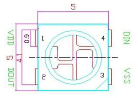
The WS2812B contains only 4 pins, 2 for supply and ground, one to receive the data DIN and the DOT pin to transmit it to the next pin.
| Pin No. | Symbol | Description |
|---|---|---|
| 1 | VDD | Power supply |
| 2 | DOUT | Control data signal output to the next LED |
| 3 | GND | Ground |
| 4 | DIN | Control data signal input |
Daisy-chain
To understand how data flows, imagine we have a strip of 3 LEDs and we want to set them to Green, Blue, and Red (in that order). The controller ‘pushes’ the data through the chain:
- First Pulse: Send Red. (LED1 is Red, others are off).
- Second Pulse: Send Blue. The Red data is pushed to LED2, and LED1 becomes Blue.
- Third Pulse: Send Green. The Red data moves to LED3, Blue moves to LED2, and LED1 becomes Green.”

Color and timing format
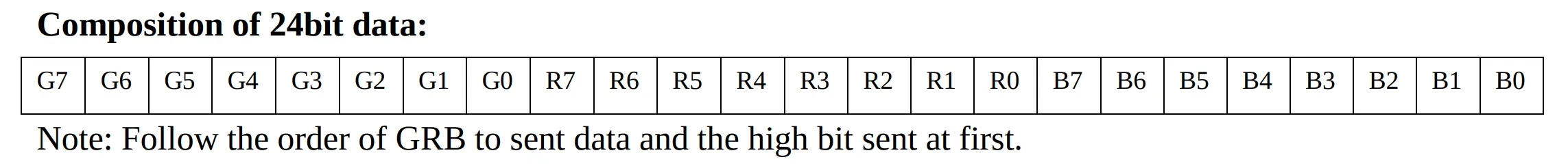
Until now we have talked about sending the color Red, Green or Blue, but we need to know the low level interface, How the bits are sent? And, how is the electronic signal looks like. The WS2812B expect the color as 24bit stream consisting in 8 bits for green, then 8 bits for red, and finally 8 bits for the blue color, sending the MSB first: First send the G7, then G6… up to B0.
The rest of required information to start developing is in the next images.
STM32
For this project I am using an STM32H523. It features the required peripherals to automate the bit streaming sending, like DMA (Direct Memory Access) and PWM.
This offloads the heavy lifting from the CPU.
While the transmission could be implemented using bit-banging (manually toggling a GPIO high and low with precise delays), this approach is highly inefficient. It consumes 100% of the CPU’s cycles just to manage timing, whereas the DMA/PWM method allows the hardware to handle the signal in the background.
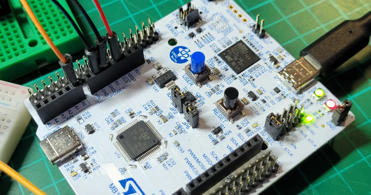
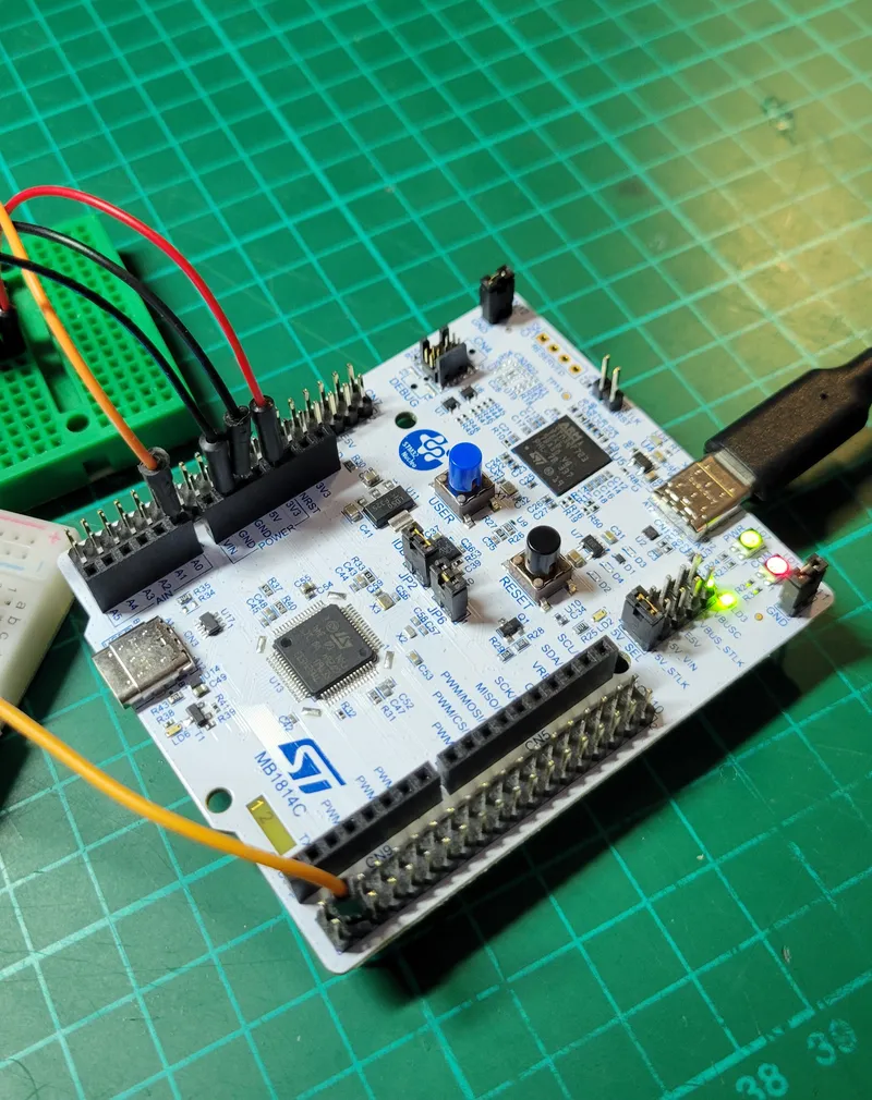
For this example I am using a NUCLEO-H533RE connected directly to the DIN of a WS2812B.
Configuring Timer
The pulses required to drive the WS2812B closely resemble a PWM signal. The PWM (Pulse Width Modulation) signal is a rectangular wave with a firex period(T).
It consist of a portion of time where the signal is High and the remainder where it is Low; this relationshit is known as Duty Cycle typically expresed in percentage.
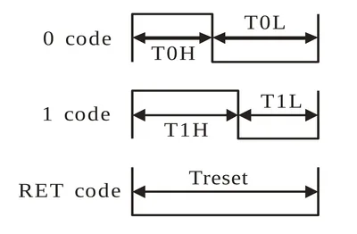
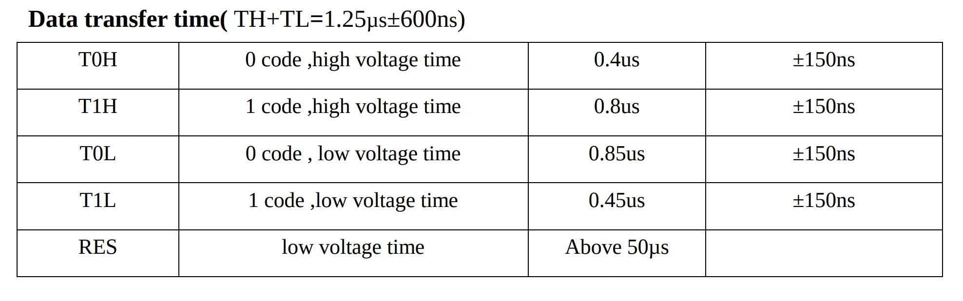
From the timing table, we know that:
- The Period of the signal is 1.25 us.
- When we send a 1, the High will be 0.8 us.
- When we send a 0, the High will be 0.4 us.
- To reset the stream, a low of 50 us is required.
The STM32 timer, when configured for PWM output, operates as a counter. For every clock tick, the timer’s value increments by 1.
The logic follows two main thresholds:
- Output Compare (OC): When the timer value matches the Output Compare register, the output signal toggles its polarity (usually switching from High to Low).
- Counter Period (ARR): Once the counter reaches the Counter Period (Auto-Reload Register), it resets to zero and sets the output back to High, starting a new cycle.
Note
The polarity of the output signal can be swap in the configuration.

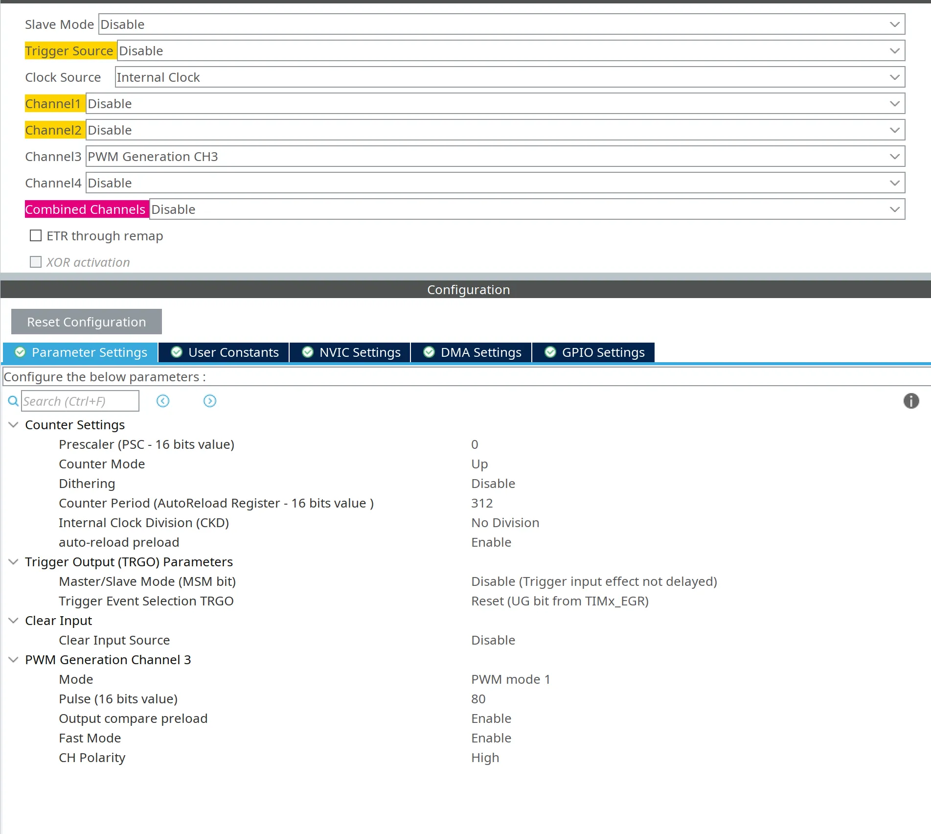
Getting the ARR and OC of the PWM.
The period of the timer depends on the clock configuration, in my case I am using the STM32H523 running at 250 MHz in all the buses.
With a clock of 250 Mhz the Counter Period, the required counter value is calculated as . Since we can only
configure an integer we stick to 312 which gives us a period of .
Using the same methods, we can calculate the counter requires for the 1’s and 0’s. The PWM output starts at low, and when the OC is reached, the level changes to High. However, for the WS2812B, the order is inverted, we need first to be in high and then change the output to low.
- For the T1H: 0.8 us is 200 pulses
- For the T0H: 0.4 us is 100 pulses
STM32CubeMX Timer configuration.
In my project, I am using the Timer 4 (TIM4) Channel 3 (CH3) but you can use the one that suits you the most providing they have PWM Generation.In my NUCLEO-H533RE this
timer and channel combiation is exposed in pin PB8.
Important
The ‘Auto-reload preload’ must be set to Enable. If it remains disabled, the DMA update to the **Output Compare (OC) **register takes effect immediately instead of waiting for the next cycle to begin. This could lead to inconsistent pulse widths and glitched colors on your LED strip.
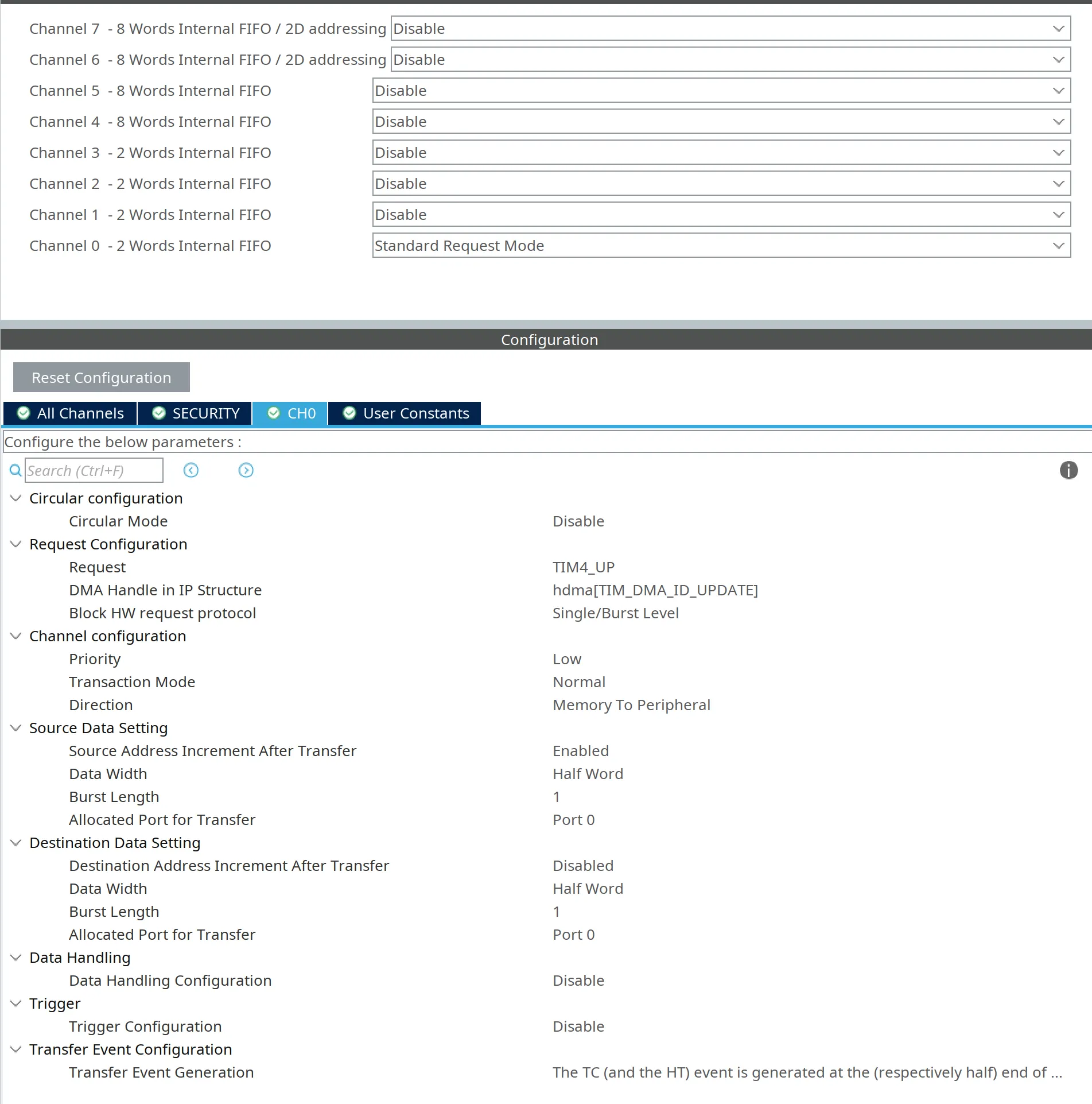
GPDMA
Since we need to send different 1’s and 0’s to the WS2812B, we need to change the PWM values (OC of the TIM4_CH3) on the fly.
The GPDMA (General Purpose DMA) peripheral is perfect for this task: once configure with the data to be send, the DMA handles the
update of the TIM4_CH3 (OC) without CPU intervention.
Warning
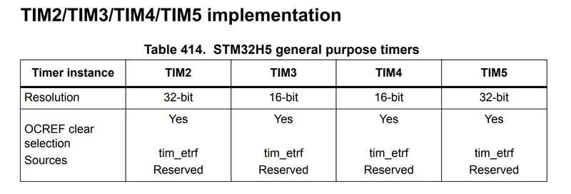
The Data width of the Source and destination settings will depend on your timer width. In the case of the STM32H523 is 16-bit width, or half-word.
The GPDMA’s role is to automatically update the Output compare (OC) register at the start of every timer cycle. This is triggered by the Update Event (UEV),
which occurs every time the timer reaches the ARR value and resets.
By using the GPDMA to preload the next pulse width value into the CCR (Capture/Compare Register), we ensure that each bit of the WS2812B stream is sent with perfect timing.
This hardware-level automation prevents the CPU from having to intervene every few microseconds, effectively eliminating jitter and timing errors. Below the cubeMX configuration
for the GPDMA can be seen.
DMA + Timer chain
To sum up, this image tries to explain how the system works from start to end. During a cycle the current OC value is used. When the cycle ends, the new preloaded value takes place in the OC register, generating an Update Event and consecuently the DMA move the next OC value from the buffer to the preloaded OC register.

Source Code implementation
With the configuration implemented in the previous sections, we can now start coding. First generate the code using cubeMX and then we can start adding our custom code to prepare the WS2812B data.
Preparing the RGB information
Before sending any color, we need to adapt our RGB color to the format expected by the WS2812B. We need to generate 24 bits (8 bits per color) that we will pass to the DMA. Since the DMA is writting directly to the OC register, we have to transform the RGB colors to the Output Compare values.
#define T0H 100#define T1H 200
// RGB structtypedef struct { uint8_t g; uint8_t r; uint8_t b;} Rgb;
void genData(Rgb *rgb, uint16_t *wsData, uint32_t numLeds) { for (uint32_t led = 0; led < numLeds; led++) { // Get the RGB for led. Rgb color = rgb[led]; uint32_t baseOffset = led * 24;
for (uint32_t bit = 0; bit < 8; bit++) { // Write the green bit starting by G7 wsData[baseOffset + (7 - bit)] = (color.g & (0x1 << bit)) ? T1H : T0H;
// Write the red bit (be aware of the +8 offset in the array index) wsData[baseOffset + (7 - bit) + 8] = (color.r & (0x1 << bit)) ? T1H : T0H;
// Write the red bit (be aware of the +16 offset in the array index) wsData[baseOffset + (7 - bit) + 16] = (color.b & (0x1 << bit)) ? T1H : T0H; } }}Be aware, that in order to restart the WS2812B, a reset signal of 50 us is required. So in the final code, we should append 0 value at the end, so the GPIO stay low when the timer ends.
Seding the data using DMA and Timer.
With the data adapted to the Output Compare register, we can start the DMA.
// Change to your channel#define DEST_DMA (uint32_t)&(ws->init.tim->Instance->CCR3)#define NUM_LEDS 1#define NUM_BITS_PER_LED 24
void main(){ // ... Autogenerated code ... Rgb color = {50, 0, 0};
// Start timer. HAL_TIM_PWM_Start(&htim4, TIM_CHANNEL_3);
// pwmData for only one led. uint16_t pwmData[NUM_BITS_PER_LED * NUM_LEDS + 1]; pwmData[NUM_BITS_PER_LED * NUM_LEDS] = 0; // Set last bit to always low.
while(1) { // some weird pattern color.g = color.g ? 0 : 50; color.r = color.r ? 0 : 50; color.b = (color.b + 1) % 50;
genData(&color, pwmData, NUM_LEDS); // one led
__HAL_TIM_ENABLE_DMA(&htim4, TIM_DMA_UPDATE);
HAL_DMA_Start_IT(&handle_GPDMA1_Channel0, (uint32_t)wsData, (uint32_t)DEST_DMA, numBytes);
HAL_Delay(1000);
}
}