
The objective
There are plenty of full application examples and tutorials for the STM32N6570-DK. However most of them are step-by-step tutorials, without a proper explanation for the selected peripheral configuration. Therefore I wanted to work on working with the LCD-TFT Display Controller the LTDC.
My main objective is to basically: learn to interface an LCD display (the included in the STM32N6570-DK), configure and use the LTDC peripheral. I want the final software to have the framebuffer stored in ram (a simple array) and get the screen to update the displayed information based on the array contents, automatically without software intervention.
The STM32N6-DK
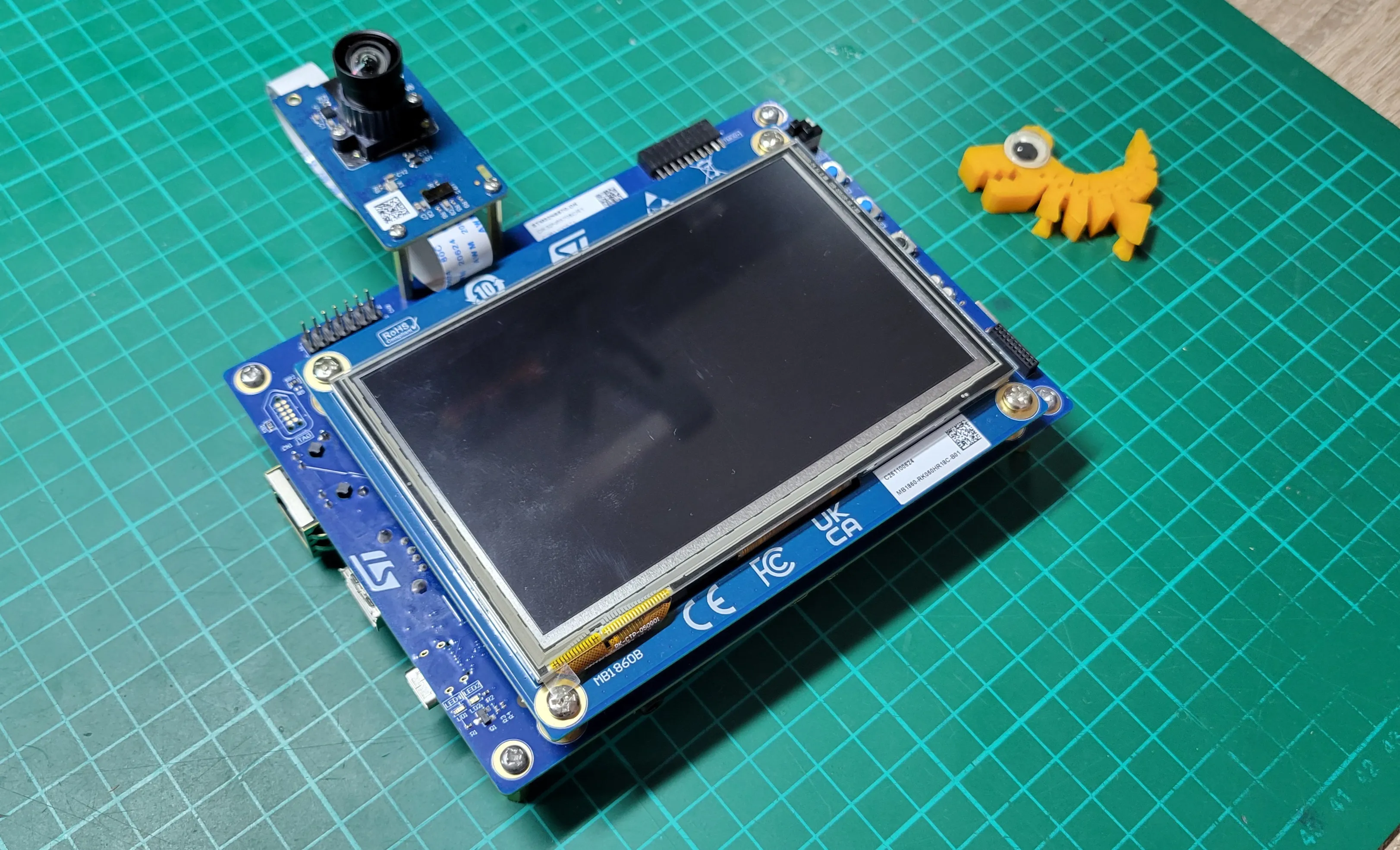
For this test I am using the STM32N6570 Discovery Kit (ST Page) which includes a five inch LCD with capacitive touch panel, and a camera board (MB1854B IMX335). I will work with a basic FSBL and do the actual work in the Secure Application code, if you want to work with Non-Secure Application is up to you, but you will need to adapt the RIF.
Reference documents
| Ref | Name | Link | Desc. |
|---|---|---|---|
| [1] | STM32N657 Discovery Kit - User Manual | UM3300 | For Discovery kit pinout, connectors and internal interfaces. |
| [2] | STM32N6 - Reference Manual | For the detailed information about the peripherals, registers, and programming required data. | |
| [3] | STM32N6 - Datasheet | For technical related description: clock speeds, voltages, and so on. | |
| [4] | RK050HR18-CTG_DS_001 | Datasheet | LCD Screen of the discovery kit screen |
Debug configuration: UART
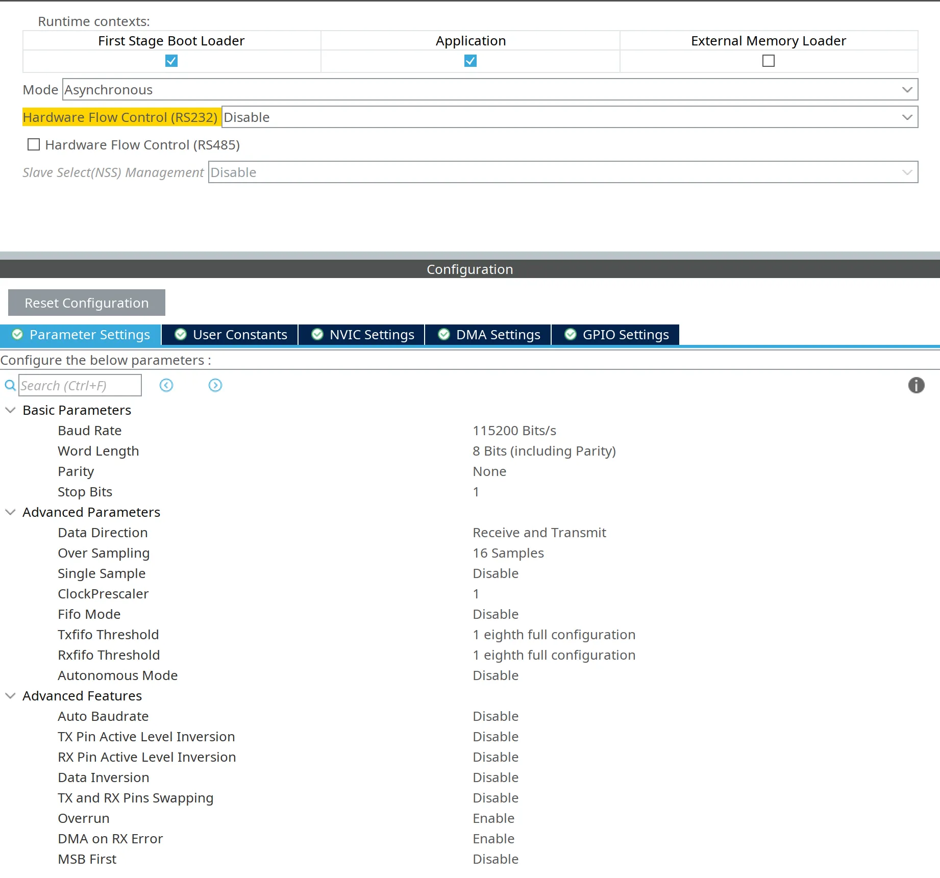
In order to debug the application, I am configuring the UART to send string information back to the Host computer. The board has the UART1 (PE5/PE6) directly available as a virtual COM port using the STLINK, so we are using it for basic debugging. You can also disable all the unused peripherals.
Important
Remember to assign the GPIOs (PE5/PE6) to the Application in the GPIO section.º
The UART is configuring according to the User Manual[1] (7.19):
- 115200 bit/s
- 8-bit data
- Even parity
- One-stop bit
- No flow control
LCD-TFT first steps
The STM32N6570-DK comes with a five inch LCD screen, the screen is a RK050HR18H-CTG with a resolution of 800x480.
The LCD is connected through the CN3 connector of the discovery kit which connects directly to the LTDC (LCD-TFT Display Controller) peripheral of the STM32N6. The LTDC can be used to increase the system performance since the LTDC can read the buffer directly from the RAM and update the screen without CPU intervention.
Note
There is a more detailed explanation of the LTDC working modes in LTDC Introduction document
We are using the LTDC to draw a framebuffer, located in internal SRAM (AXISRAM1/2) to the LCD screen. Since we are not using any UI library, we will focus on just understanding the frame updating with simple colors.
CubeMX: LTDC Peripheral configuration
The LTDC peripheral is located for the STM32N6 configuration under the Multimedia section. Once activated, the first box allows us to select the display type and, since we have the 24 lines connected to the LCD connector (R0-7, B0-7 and G0-7), we have to select the RGB888 interface. Also assign the LTDC to the Application environment.
![LCD Interface definition in [4]](/_astro/LCD_InterfaceRGB.BJkIJSGp_Z15w3Xf.webp)
Now , let go though the configuration tabs: Features, NVIC Settings, GPIO Settings, Parameters Settings and Layer settings.
Features
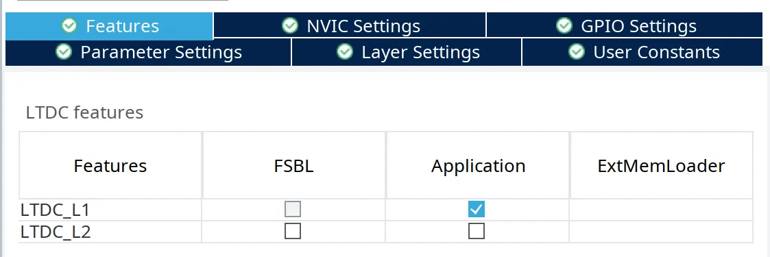
The Features tab list two items, the LTDC_L1 and LTDC_L2, which correspond to the layers of the LTDC. These layers contain the framebuffers
that can be shown or blended together, using an alpha channel (transparency).
This can be use, for example, to have one frame buffer (L1) with the constant UI display information with a transparent area, and then the second layer, with the framebuffer that is fed from a camera. Having a final image of the two framebuffers mixed. This blend, or combination is performed automatically by the LTDC peripheral.
Note
You can find more information in section 4.3 of the LTDC Introduction document
Since I want the simplest example, I will only use Layer 1 to draw something, so I assign he LTDC_L1 layer to the Application.
NVIC Settings
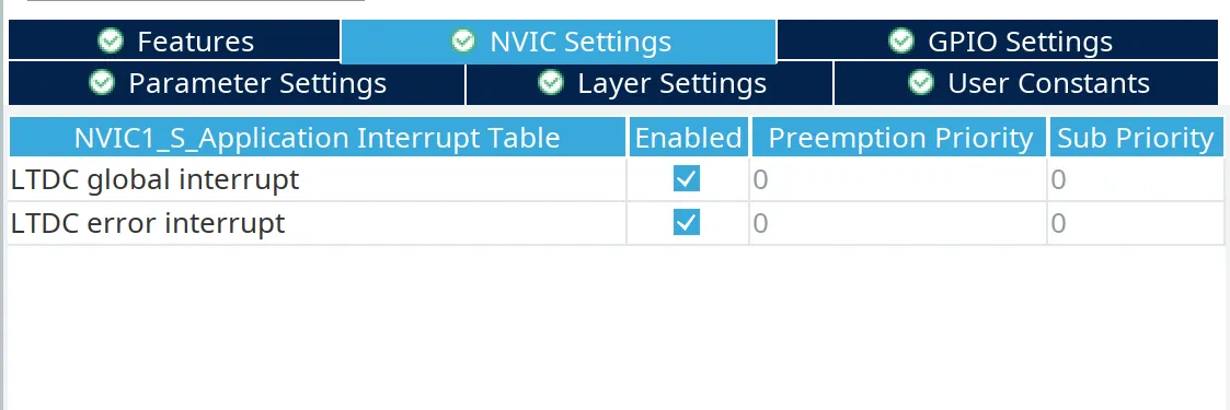
This tab is also pretty self-explanatory with the two sources of interrupt of the LTDC controller. In our case we want both the IRQs enable.
GPIO Settings
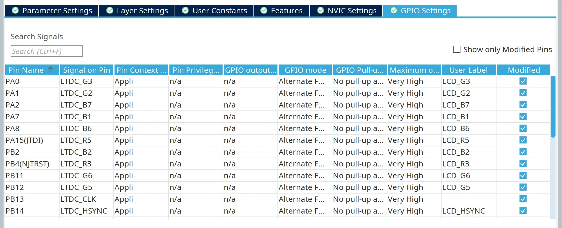
The GPIO setting shall be automatically filled. There are some changes that I made to make this works. The first critical step is to assign all the GPIOs to the Application context, otherwise, even they are configured wont be used by the Application.
Also, since we are dealing with fast and critical signals, I changed all the GPIOs’ speed to Very High.
Parameters Settings
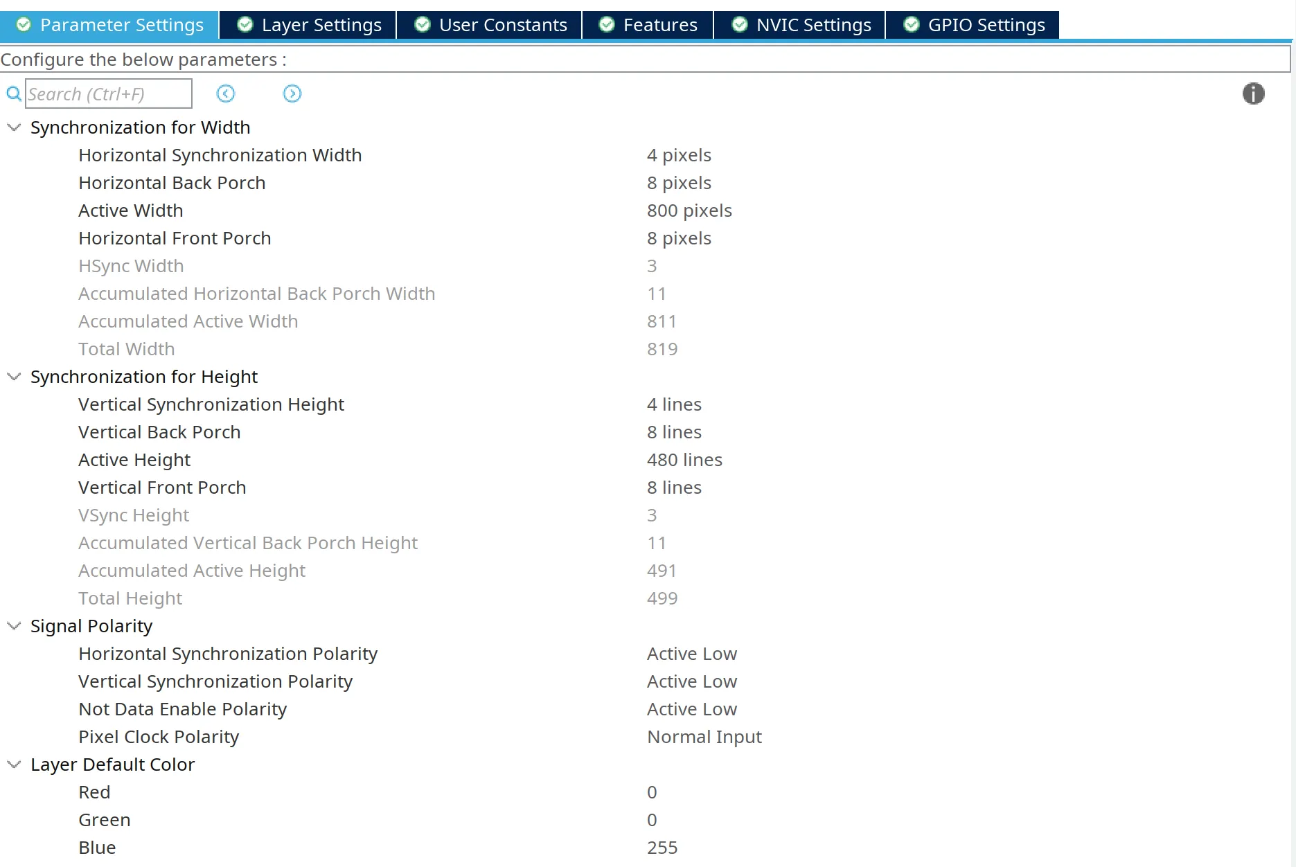
The parameters settings tab is probably the most confusing one, at least for me, when starting to work with LCD screens. I wont go much into details, but I will point to to you where to find the correct information in the screen datasheet for each LCD.
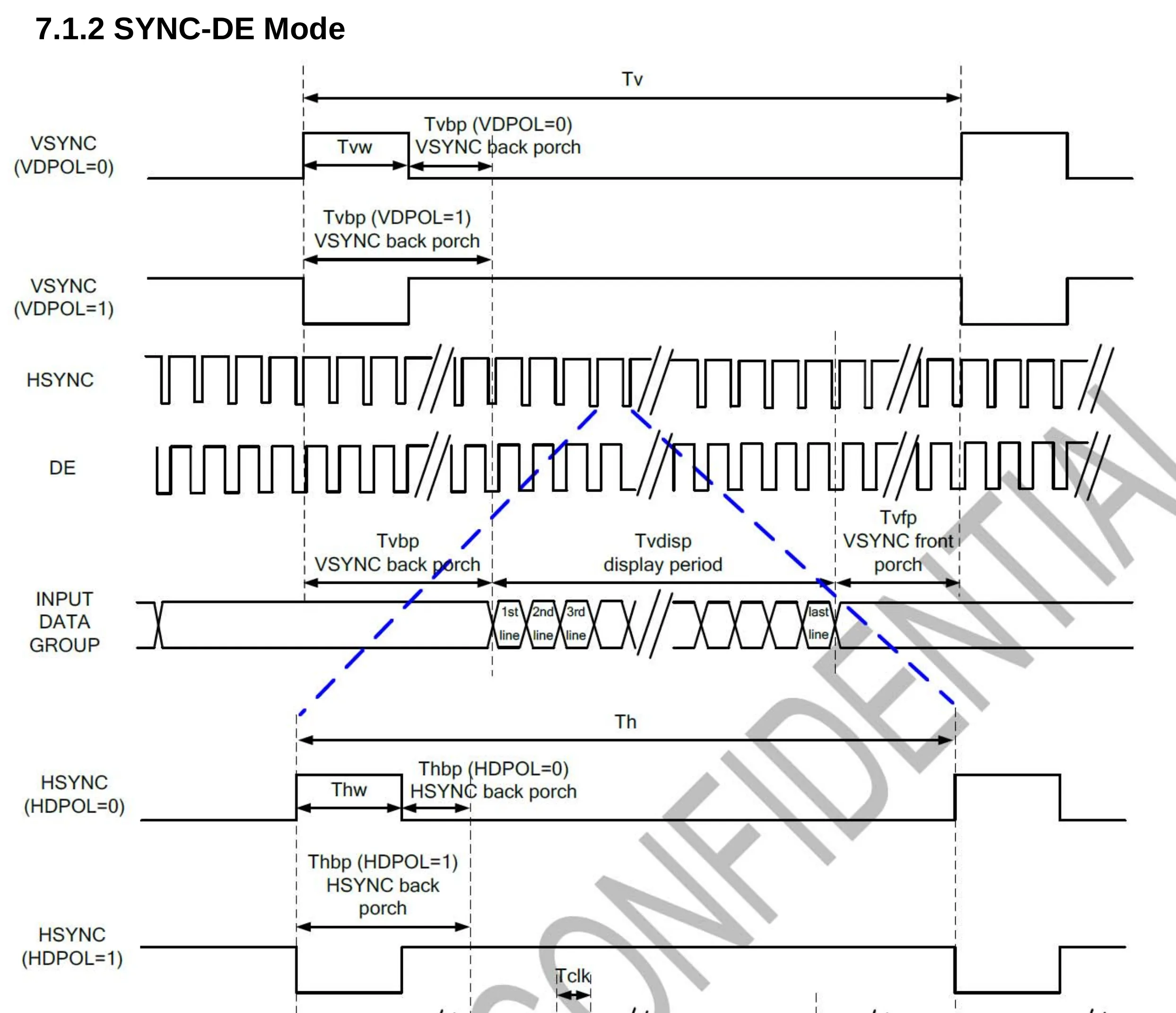
We need to fill the synchronization data for the Width and the Height. Let’s start with the easy ones, Active Width and Active Height which are the
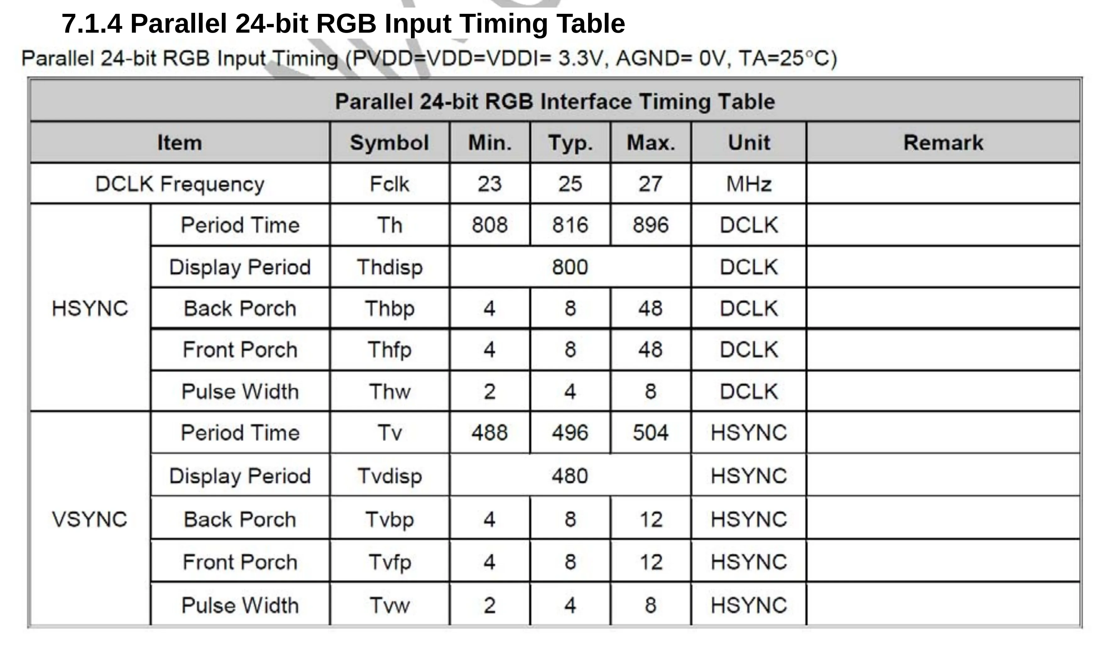
display width and height: 800 and 480, which correspond to the Thdisp and Tvdisp in the datasheet.
Then the porches, nothing fancy:
- Horizontal Back/Front Porch =
ThbpandThfpwhich are 8 and 8. - Vertical Back/Froint Poch =
TvbpandTvfpwhich are also 8 and 8.
The synchronization width and Height correspond to the Pulse Width for the HSYNC and the VSYNC fields in the datasheet.
The next steps are the clock polarities which can be obtained from the signal diagram of the LCD datasheet [4].
From the diagram below, the VSYNC and HSYNC signals depend on the value for VDPOL and HDPOL respectively.
And these two values, VDPOL and HDPOL, depend on the LCD driver. The LCD driver of the RK050HR18 screen is a ST7262-G4 (from the LCD datasheet) and from the driver
datasheet we can see that by default VDPOL and HDPOL are set to ‘1’, since the register default value is 0xD7.
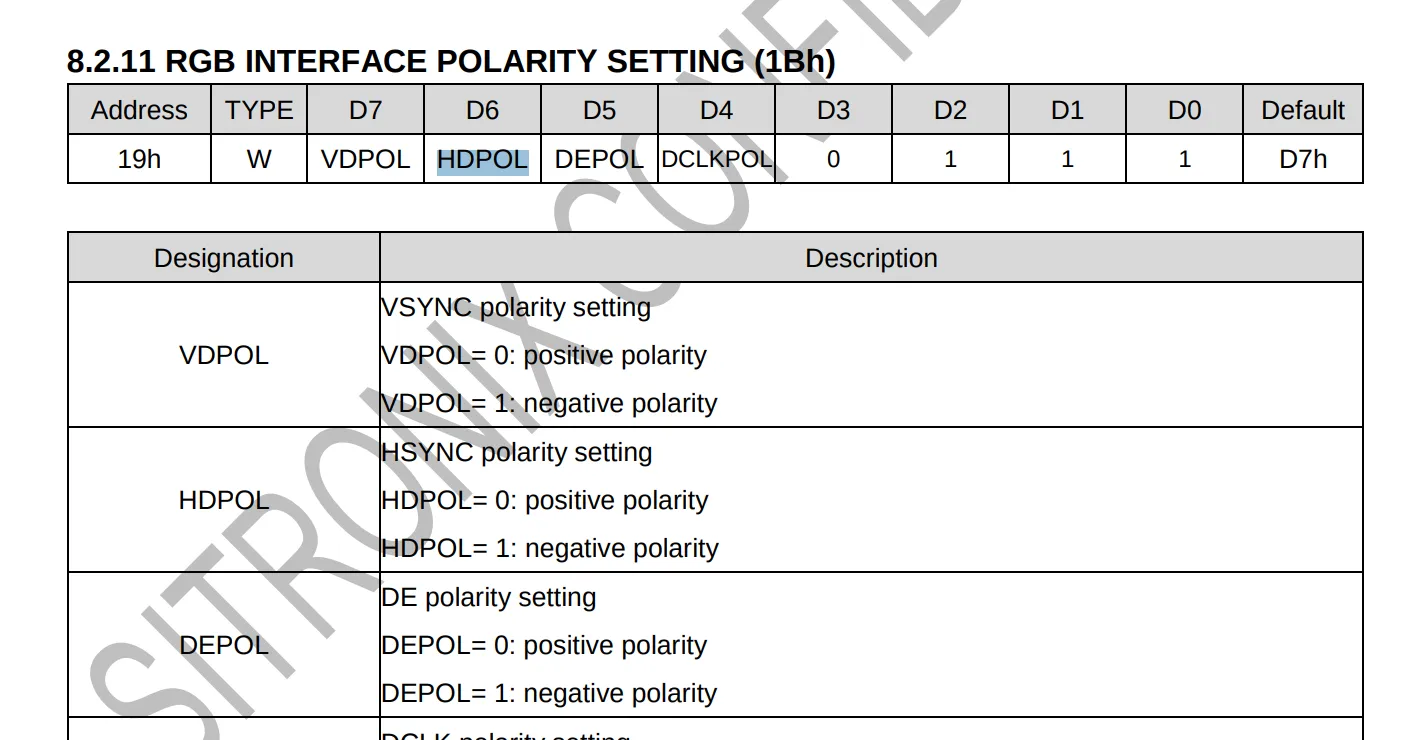
Therefore the values for the clocks are all Active Low and Normal Input for the clock.
Layer settings.
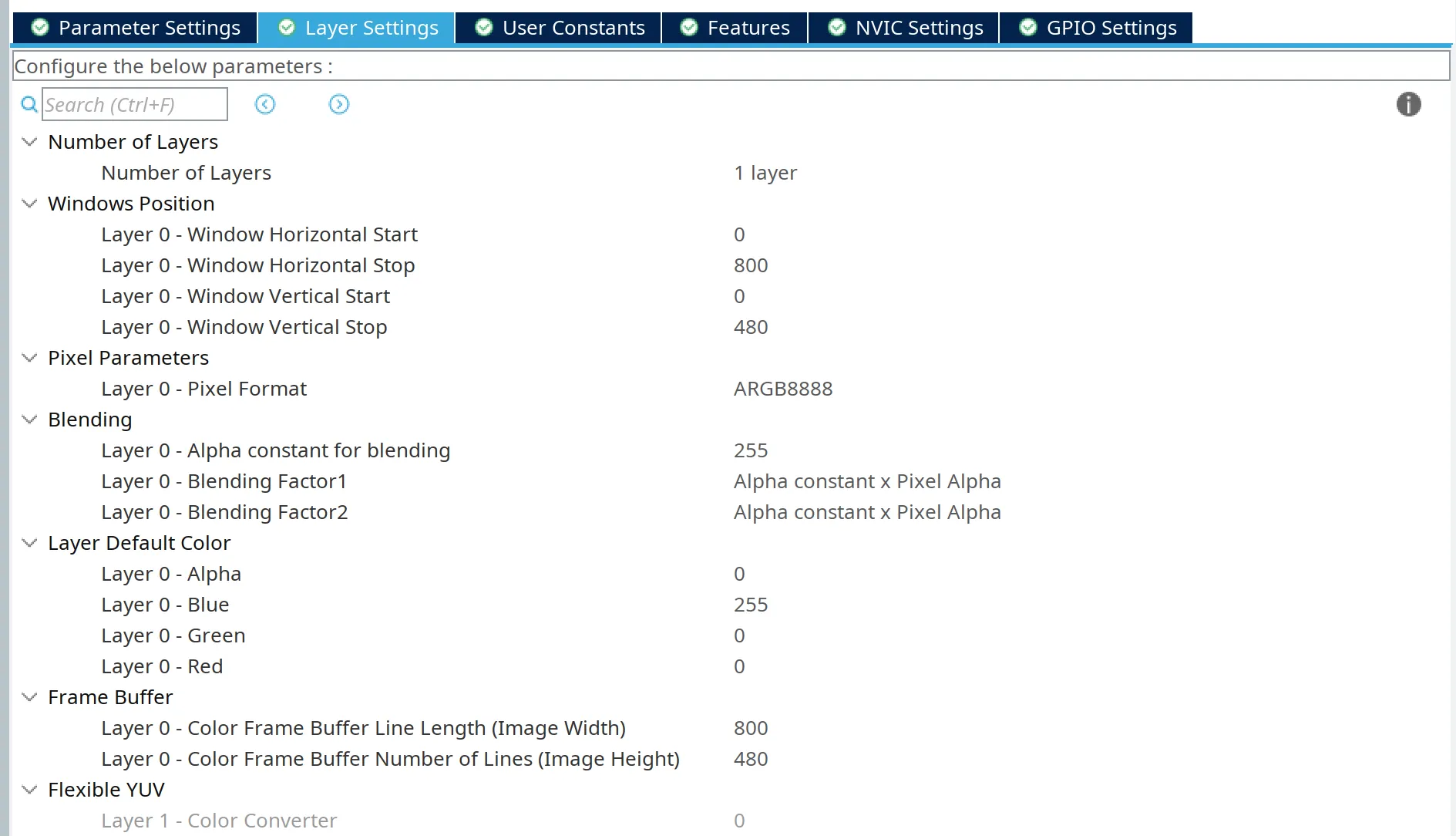
This tab contain the information about the layer. Since we are using a screen with 800x480 resolution, and we want a layer that cover all the screen, we would need to cover the whole window and therefore we want the Window position from 0 to 800 in the horizontal direction, and 0 to 480 in the vertical direction. The same goes for the Frame Buffer option at the bottom.
For the pixel format, we will use ARGB8888 which has 8 bits for red, green and blue, plus the first byte assigned to the transparency. I used
this format for convenience since a pixel is now 32-bit wide, which can be stored perfectly in an uint32_t.
For the blending, I am actually not using it, so leave as seen in the image.
The default color for the layer can be used to check that the screen is actually working. By selecting a color different from the black, if the LTDC is working, a color will be displayed, even with a misconfiguration in the RIF or the framebuffer address.
Extra GPIO Configuration
On top of the already configured GPIOs in the LTDC screen, we have to add some extra pins required by the interface. The TFT LCD Connector (CN3)
of the STM32N657 has the LCD_ON/OFF (PQ3) and LCD_BL_CTRL (PQ6) signals that are not handled by the LTDC. These two pins control the ON/OFF
of the screen and the backlight.
These two GPIO have to be configured in the GPIO section, and will be managed by usual HAL_GPIO_Write functions.
CubeMX: LTDC Clock configuration
![LTDC Clock. Image from STM32N6 Datasheet [2].](/_astro/LTDC_Clock.CzB2TYrR_ZfDoti.webp)
We have finally completed the LTDC configuration. However, as any other peripheral, the LTDC requires a clock to work.
The main clock is obtained from the pclk5 which is the APB5 Clock, but the interesting part is the pixel_clk signal.
That signal is the clock used by the LTDC to drive the actual LCD screen clock and from the timing table from the LCD dataheet (image below),
the clock signal (DCLK Frequency in the table), the clock shall be set to 25 MHz.
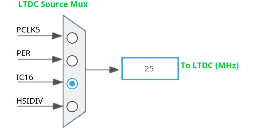
In order to achieve the 25 MHz, we will generate the clock from ic16_ck since all the “normal” clocks in the N6 have values in the hundreds of MHz, but
the ic16_ck has a divider to slow down the associated clock.
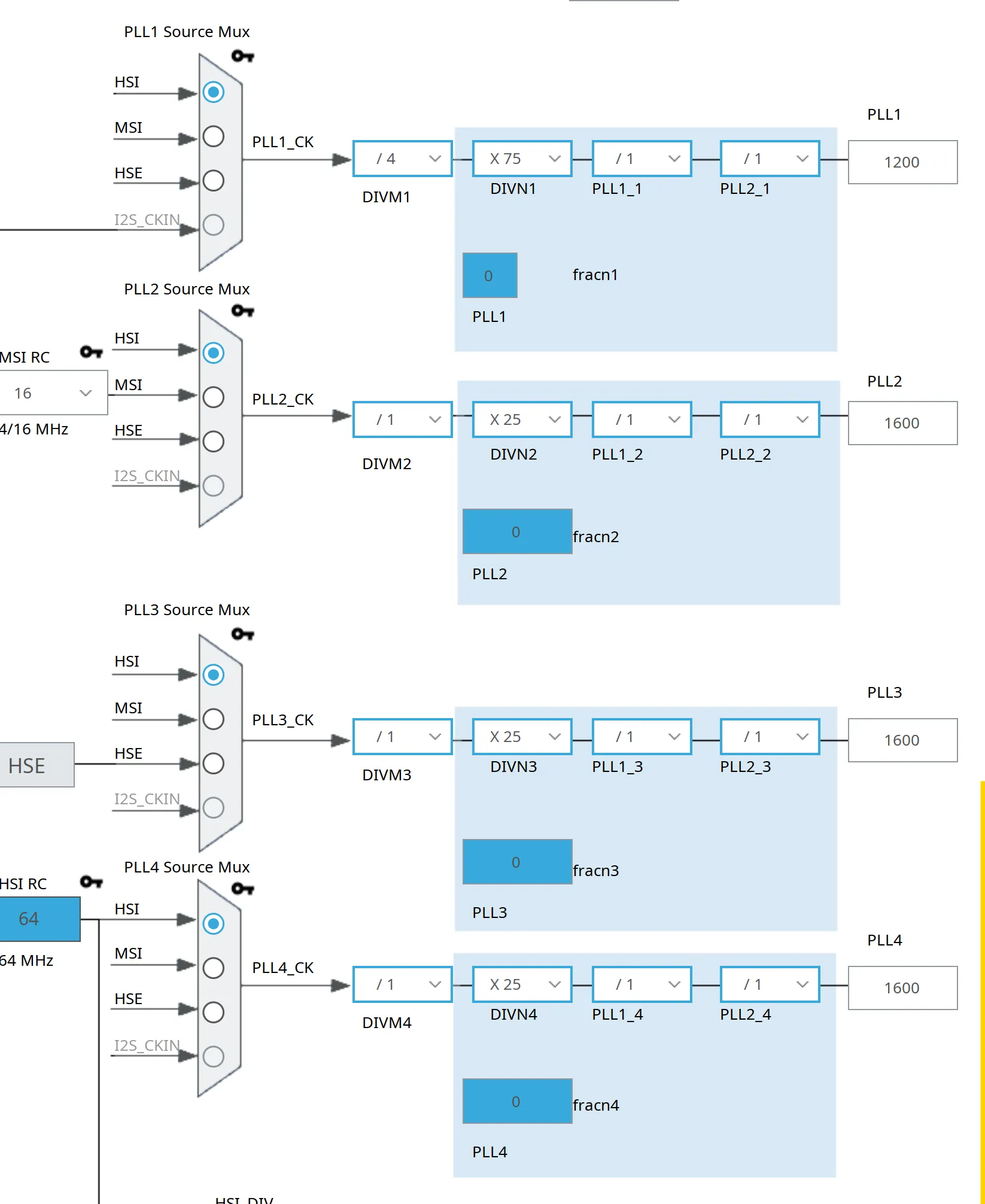
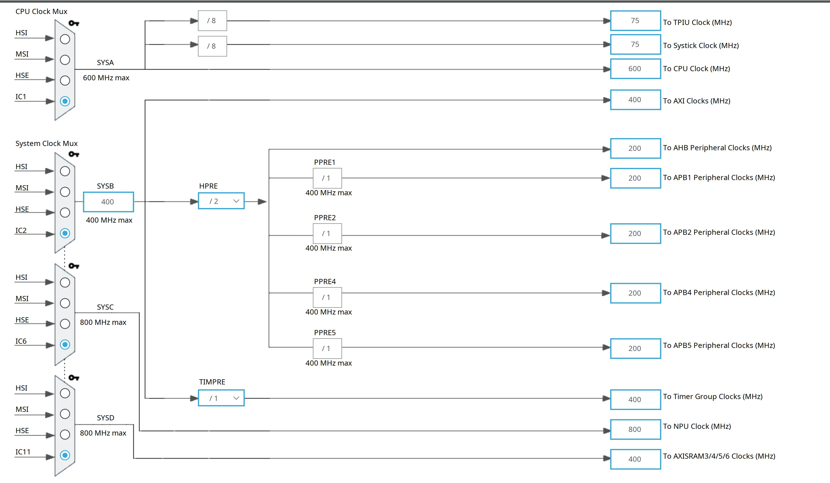
I wont go into much detail about clock configuration, I just leave the configuration required to work with the LTDC and generate a 25 MHz signal for the pixel_clk.
PLL Configuration
IC16 and LTDC Clocks

CPU, AHB and APB clock
CubeMX: RIF
We have finished configuring the LTDC peripheral and the required clocks. However, if you try to write something to the framebuffer of the LTDC you will find
that only the background image is seen, and no data is updated. This is due to the RIMU box in the diagram below.
![Display Subsystem diagram from the datasheet [2]](/_astro/DisplaySubsystem.DBtL_5f1_Z1HUhxf.webp)
The RIMU(Resource Isolation Master Unit) box is part of the RIF (Resource Isolation Framework), a system that enforces and manage the isolation of STM32 resources and peripherals.
Since the LTDC has direct access to the framebuffer through the AXI bus, the LTDC has to read directly from the AXISRAM (in our example, you can change the location of the framebuffer), and there is RIMU box between the LTDC and the AXI bus, we need to configure the RIMU to allow the communication.
This is done by first enabling the RIF in CubeMX -> Security -> RIF and assign it to the Application.
CubeMX: RIF tab
Then move into the RIF Tab at the top of CubeMX. Here we have a Peripheral (RISUP) and Domain (RIMU) section.
In the Peripherals, we have to add privilege to the LTDC_CMN and LTDC_L1 items and then in the Domain tab, check the Secure and Privilege
boxes for the LTDC_L1.
The Source code
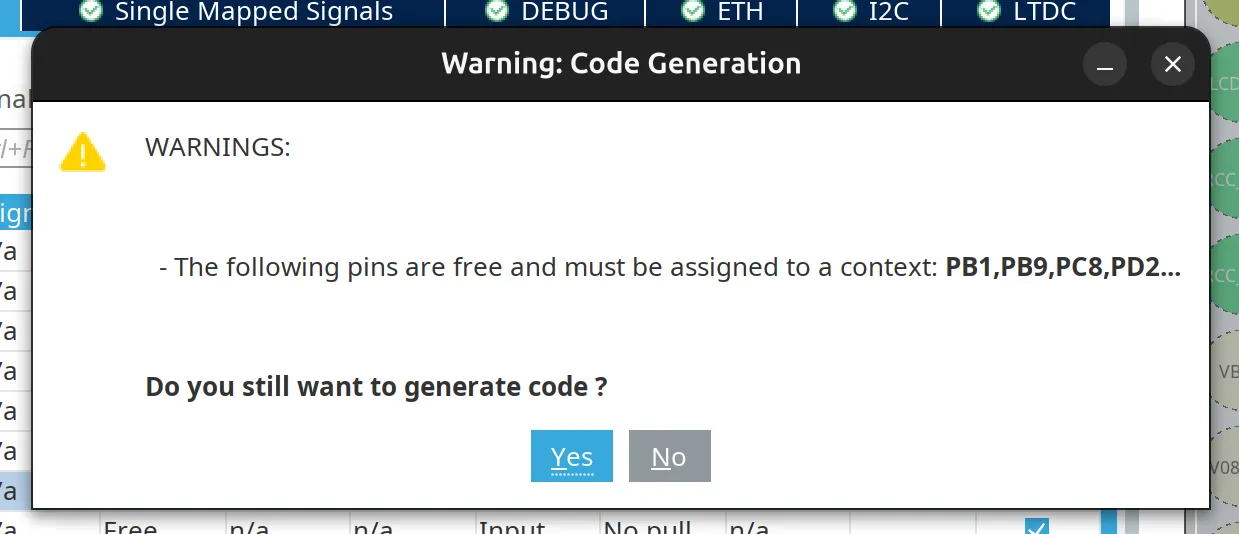
With all these steps, we are finally there and can generate our source code. There will be probably a warning with the “The following pins are free and must be assigned to a conetext: …”.
This message appear if CubeMX pre-configured all the pins used in the STM32N657-DK. Since we are focusing only in the LTDC, most of them are just left without assigning to any context (FSBL or Application).
The final change is adding our framebuffer to the source code and connect it to the LTDC Layer. The framebuffer is just an array of 480x800 pixels, since each pixel is 4 bytes-wide we can use
the uint32_t type to store all the information of a pixel.
Keep in mind this is a demostration only, and only this buffer will fill 1560000 bytes of RAM, almost the whole AXISRAM! In future projects this framebuffer shall be moved to PSRAM or external RAM.
// ...
/* Private user code ---------------------------------------------------------*//* USER CODE BEGIN 0 */
// Create the image buffer and fill it with zeroesuint32_t image[480 * 800] = {0};/* USER CODE END 0 */
// ...The next step is to assign the image buffer to our LTDC Layer. The LTDC register are shadowed, that means, that even you change the values, the actual used
register values in the peripheral are not updated. In order to force the LTDC to get the register values and use them is by forcing a layer/global reload.
// ...
/* USER CODE BEGIN 2 */
HAL_GPIO_WritePin(GPIOQ, GPIO_PIN_3, GPIO_PIN_SET); /* LCD On */ HAL_GPIO_WritePin(GPIOQ, GPIO_PIN_6, GPIO_PIN_SET); /* 100% Brightness */
HAL_LTDC_SetAddress(&hltdc, (uint32_t)image, LTDC_LAYER_1); HAL_LTDC_ReloadLayer(&hltdc, LTDC_RELOAD_IMMEDIATE, LTDC_LAYER_1);/* USER CODE END 2 */
// ...And finally, modify the buffer in the main loop to see the screen changing.
// ...
/* Infinite loop *//* USER CODE BEGIN WHILE */ uint32_t cnt = 0;
while (1) { for (uint32_t i = cnt; i < cnt + 400; i++) { uint8_t val = (uint8_t)(((i - cnt) * 255) / 399); imagen[i] = 0xFFFF0000 | (val << 16) | (val << 8) | val; }
cnt += 400; cnt %= 480 * 800;
/* USER CODE END WHILE */
/* USER CODE BEGIN 3 */ } /* USER CODE END 3 */
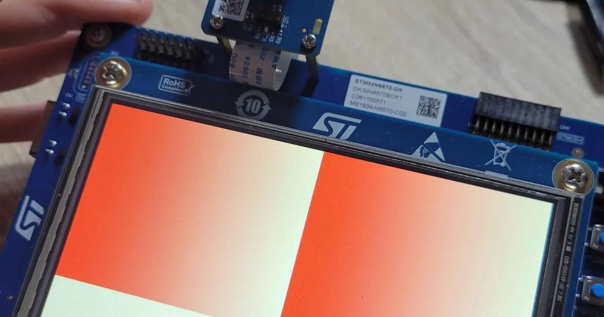
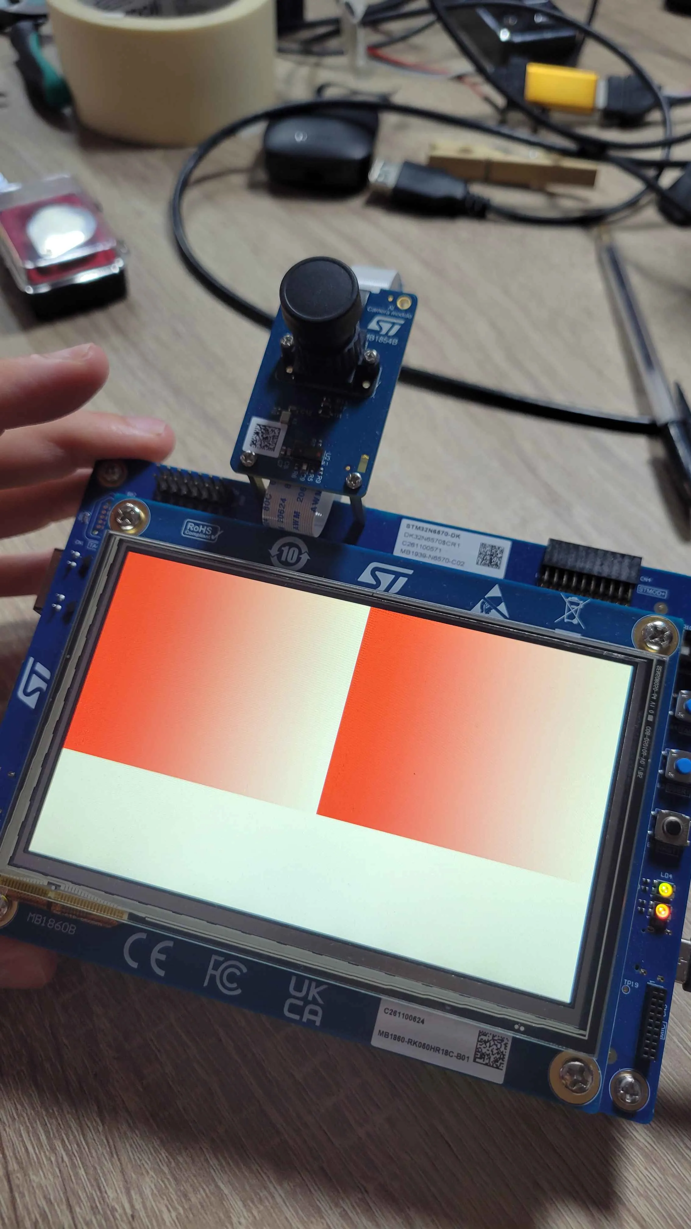
// ...And here you have the final result! the display is working and displaying a red gradient!
If you make it here, thank you very much! I hope you learn something new today! If you feel to contribute you can also buy me a coffee!
Dont forget to follow in my other social networks!